By Dan Martin
How to Reach Grid Parity
Grid parity for solar power is the point at which the installed cost of electricity produced by solar panels is equal to or cheaper than electricity produced by traditional fossil fuels. Once grid parity is reached, demand for photovoltaic products will dramatically expand as market-based behaviors rapidly displace fossil fuel power sources. Grid parity will be achieved first in those areas of the world that have a combination of abundant sunshine and comparatively high grid electricity prices, places like California, the U.S.A., and Japan. The fastest way to grid parity is through efficiency improvements and cost reductions in Photovoltaic (PV) cell and module manufacturing.
Learning Curve theory
Learning curve theory states that as the quantity of items produced doubles, costs decrease at an often predictable rate. The learning curve assumes that as volume increases, costs of raw materials will decline, manufacturing efficiency will improve, administrative and distribution costs can be spread over higher production volumes, and other economies of scale can be realized. For most industries, the learning curve is between 15%-25% (meaning that as volumes double, costs will decrease by 15%-25%). A faster learning curve for the solar PV industry will reduce the time to grid parity. So, what is the learning curve for PV and what can the industry do to accelerate it?
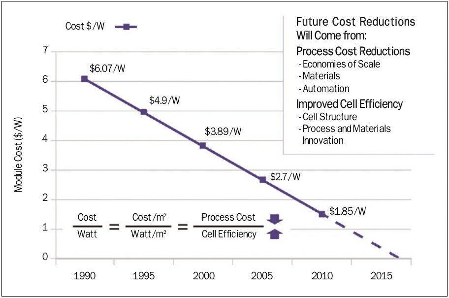
Figure 1. PV RPT cost per watt (Source: SEMI PV Group)
PV Learning Curve
Figure 1 illustrates the PV industry learning curve over the past several years. It is this industry learning curve that will be the primary contributor to reaching grid parity in most parts of the world over the next 2 to 8 years. This total cost per watt reduction is a summation of all the costs that go into module production: raw material costs, yield, equipment costs, factory utilization, shipping, and etc. The cost per watt also is comprised of cell efficiency. The experience curve or learning affects since 2000 for the PV industry based on this data are around 80%-85% (a 15-20% cost reduction with every doubling of industry output) is about the same as many other industries, such as aerospace, shipbuilding and machine tools. Good, but not great. Recent cost reductions have been primarily driven by the worldwide recession and steep price cuts. How can we accelerate sustainable cost reduction?
One way to accelerate the learning curve is through technology developments. Governments around the world are funding research and development efforts that will hopefully yield results that will eventually reach the marketplace and our rooftops. Individual companies are also investing in R&D to improve cell efficiencies, knowing that the lowest cost per watt in a particular application will lead to market share gain.
But industry-wide learning curve affects do not generally depend on major technology breakthroughs. In the solar industry, since 1990, we see a steady stream of incremental efficiency improvements, not major breakthroughs. In fact, the average cell efficiency gain across all solar technologies is only about 25% over the last 15 years (U.S. National Renewable Energy Lab “Best Research-Cell Efficiencies” scorecard). The following chart summarizes the cell efficiency improvements by NREL for select technologies since 1990.
If technology developments have delivered only 25% of the cost reduction in the 1990-2005 time frame, where is the remainder of the observed cost reductions in solar PV coming from (around 175% over the comparable period)? Much of these costs reductions are due to manufacturing efficiencies, typically from materials cost reductions, yield improvements, and throughput increases. As the solar industry has grown, suppliers have delivered faster, more efficient equipment, higher quality materials, and smarter materials usage. These gains can be further accelerated through industry roadmaps and manufacturing standards that reduce costs and focus R&D dollars on innovation. The semiconductor industry provides a useful benchmark for the PV industry in roadmaps and standards, not only because of the shared supplier and technology base (PV cells are, in fact, semiconductors), but also because of an industry-wide agreement to achieve accelerated cost reduction at the lowest possible cost.
A Moore’s Law for PV?
The progress made by semiconductors in cost reduction is one of the technological marvels of our time. Since 1975, the cost of one transistor has been reduced by a factor of about 4,000,000. To put this into perspective, if you use the average cost of a transistor in 1976 and you take the number of transistors inside an Apple iPod, the device today would cost one billion dollars and be the size of a building.
This achievement has often been ascribed to Moore’s Law, the prediction that the number of transistors that can be placed inexpensively on an integrated circuit would double approximately every two years. As the size of transistors has decreased, the cost per transistor has declined as well, pretty much at the same rate. Moore’s Law is not a law of physics, or chemistry, or even science. It is a very, very useful observation about the rate of technology advancement in the semiconductor industry. It is also a shared objective among many members of a diverse supply chain. The most prominent characteristic of this shared agreement to achieve Moore’s Law, has been the industry-wide development process characterized by the International Technology Roadmap for Semiconductors (ITRS) and industry standards, including SEMI industry standards.
International Technology Roadmap for Semiconductors (ITRS)
The ITRS document describes the technological targets required to achieve Moore’s Law over numerous areas from research design, to photolithography, materials, and other parameters. It is updated annually and provides a technology forecast over a rolling 15-year timeline. It has thousands of contributors and pages and used by hundreds by companies in all regions of the world. Many see the ITRS process as an effective way to identify and target key requirements and “Innovation is spurred by identifying requirements.” The open and public process fosters a healthy “beat the roadmap” behavior by the industry. Some see the PV industry as very much a “parallel universe” to semiconductors who can benefit from the experience of the ITRS.
Chips vs. PV
There are both similarities and differences between the critical roadmap issues in chips and PV. Both involve substrates, interconnects, absorber/efficiency, metrology, packaging, and test. Both have common business drivers such as cost reduction, throughput, quality and reliability, and sustainability. Roadmaps can effectively identify technology gaps and serve as “learning tools for the industry” With more exposure on the critical technology gaps, more focused and cost effective innovation can occur. PV is clearly different from chips, however, and does not have the powerful organizing paradigm of the next process node that helps ground the semiconductor roadmap.

Roadmaps/Standards
Industry standards also have a close relationship to technology roadmaps. It has been said that “roadmaps without standards don’t work” Roadmaps are the group view of the technology path over time. Standards are the tools the industry uses to identify the set of specifications that define industry requirements. In other words, standards define where the industry collaborates, and roadmaps establish where the industry competes. Several studies have identified billions of dollars in industry costs that the semiconductor industry has eliminated with standards. Are there similar costs in the PV industry that can be reduced with a smart standards effort and gets us closer to grid parity? Many believe there are.
The PV industry is just starting to address roadmaps and standards. Several manufacturing standards have already been adopted by the industry and there is a growing participation of key constituents in the standard process. Active PV standards committees are in place in North America, Europe, Japan, and Taiwan under the SEMI International Standards program, the same process that supports IC manufacturing standards. One major standard specified how different machines or processes communicate together, a fundamental requirement for the modern automated factory and huge contributor to manufacturing efficiency. The standards effort in PV appears to be well on its way to contributing to a steeper learning curve.
Roadmaps are just being considered by the industry. A recent survey of cell and module manufacturers, equipment and material suppliers, and other key players ranked lack of industry roadmap and effective collaboration second behind government polices as a key barrier to industry growth. However, some industry participants believe it is too early for a technology roadmap and that engaging in an open, public dialogue could be harmful. Collaboration opponents object that roadmaps cannot define industry growth in such a dynamic market environment.
These are complex issues for the industry to consider, involving fundamental issues of competition and cooperation. Discussions are underway between key stakeholders around the world trying to identify areas where cooperation makes sense. As these discussions continue, the industry has the opportunity to learn from the semiconductor industry and find its own path, to find its own Moore’s Law that drives down costs and accelerates grid parity, enabling a great solar era unsupported by government incentives.
Dan Martin is Executive Vice President of SEMI PV Group (http://www.pvgroup.org/).
For more information, please send your e-mails to pved@infothe.com.
ⓒ www.interpv.net All rights reserved
|


.jpg)