By Charlie Gay

 As the need for clean energy increases, engineers are working to expand production and improve the efficiency of crystalline silicon (c-Si) solar factories. Five years ago, a 30 MW solar fab was a competitive size. Now, companies routinely plan 300 MW-scale fabs, and some are considering fabs on the scale of 3 GW over the next few years. A key driver in this increase in fab scale is the goal of producing solar modules at a cost of less than US$1 per watt. Four interrelated building blocks are key contributors to meeting this goal for c-Si PV: higher efficiency cells, thinner wafers, higher throughputs, and advances in automation. As the need for clean energy increases, engineers are working to expand production and improve the efficiency of crystalline silicon (c-Si) solar factories. Five years ago, a 30 MW solar fab was a competitive size. Now, companies routinely plan 300 MW-scale fabs, and some are considering fabs on the scale of 3 GW over the next few years. A key driver in this increase in fab scale is the goal of producing solar modules at a cost of less than US$1 per watt. Four interrelated building blocks are key contributors to meeting this goal for c-Si PV: higher efficiency cells, thinner wafers, higher throughputs, and advances in automation.
Higher Efficiency Cells
One approach to increasing cell efficiency is ‘selective emitter’ technology in which the conductance of the emitter--i.e., the n-type phosphorous-containing region on the cell front surface--is decreased over much of the cell area so as to increase photocurrent generation and is selectively increased under the front metal grid contacts so that the front metal grid makes a lower-loss contact to the underlying silicon (Figure 1). A traditional uniform emitter is a compromise between making low-loss contacts by reducing emitter sheet resistance and transmitting more photons by increasing the emitter sheet resistance. By selectively decreasing emitter sheet resistance only under the front metal contacts and increasing emitter sheet resistance elsewhere, one can simultaneously minimize contact-related resistive losses and maximize photocurrent generation.
.jpg)
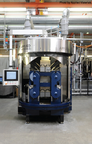
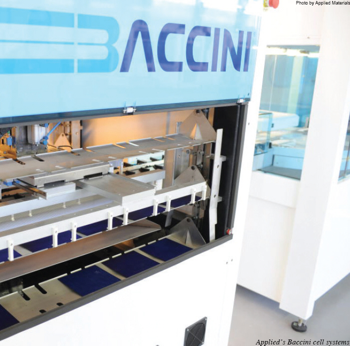
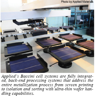
The precise local emitter doping required for an efficient selective emitter can be formed by various methods, including deposited dopants, deposited etchants, patterned wet etch masks, spatially-defined ion implantation, etc. Given that most cell manufacturers already use industrial screen printing for applying front metal grids it is convenient and cost effective for them to use closely related screen printing techniques to form the selective emitter. The key to using low-cost screen printing for selective emitter processing is to use a high-precision printer that allows one to align the front metal grid to precisely overlay the highly-doped selective emitter regions. For example, Applied Materials’sBaccini Coating Systems division offers high-volume screen printers with an Esatto upgrade that provides the required precision and repeatability. The cell efficiency gain achieved with selective emitter technology varies depending on the specifics of the cell, e.g. wafer quality, baseline diffusion process, baseline grid process, etc.; but an efficiency gain of 0.5% absolute is possible.
A key factor in optimizing the selective emitter efficiency gain is a re-tuning of the metal grid pattern so that the photocurrent and photovoltage gains are not negated by lateral ‘spreading resistance’ losses in the now-more-resistive emitter between the grid fingers. The re-tuning of the metal grid pattern generally entails decreasing the spacing between grid fingers, hence increasing the total number of grid fingers, which in turn increases the total grid coverage and decreases the cell photocurrent. The optimized balance between gains and losses is easier when using a fine-line metallization technology to make the grid.
Fine line metallization--defined broadly as methods capable of forming a continuous high-conductance grid with finger widths below 100 microns--provides stand-alone advantages including lower optical losses due to metal coverage and lower grid metals costs use due to lower paste consumption, but fine line metallization is of particular leverage when combined with selective emitter technology. There are a variety of fine line metallization technologies, including advanced screen printing, ink jet printing, aerosol printing, electroless and electroplating, etc. As with selective emitter, given that most c-Si cell manufacturers already use industrial screen printing for high-through-put metallization, it is convenient and cost effective for them to use advanced screen printing techniques such as ‘double printing’ to achieve the desired fine line metallization.
.jpg) ‘Double printing’ is simply printing a metal grid pattern, then over-printing another layer of metal exactly on top of the first to achieve a tall, narrow grid so that grid fingers shadow less (due to their being more narrow) while still conducting well (due to their being taller). Standard one-layer printing requires a relatively wide grid to achieve adequate conductance at typical layer thicknesses. Double printing increases the total layer thickness so that one can achieve equal conductance with narrower grids (Figure 2). Narrow, tall, double-printed grids cover less of the cell’s front surface so the cell has a higher photocurrent. Double-printing can be used alone to directly substitute for traditional single printing to provide an efficiency gain of up to 0.25% absolute, or can be combined with selective emitter technology for overall gains of 0.7% absolute or higher. ‘Double printing’ is simply printing a metal grid pattern, then over-printing another layer of metal exactly on top of the first to achieve a tall, narrow grid so that grid fingers shadow less (due to their being more narrow) while still conducting well (due to their being taller). Standard one-layer printing requires a relatively wide grid to achieve adequate conductance at typical layer thicknesses. Double printing increases the total layer thickness so that one can achieve equal conductance with narrower grids (Figure 2). Narrow, tall, double-printed grids cover less of the cell’s front surface so the cell has a higher photocurrent. Double-printing can be used alone to directly substitute for traditional single printing to provide an efficiency gain of up to 0.25% absolute, or can be combined with selective emitter technology for overall gains of 0.7% absolute or higher.
In all cases--selective emitter, fine-line metallization such as double printing, or combinations of selective emitter and fine-line metallization--an initial material is precisely overcoated with another material to achieve superior results. This precision overcoating requires a combination of good-quality initial coating, high-sensitivity detection of the initial material (e.g. the high-conductance selective emitter regions), precise alignment of the second patterned coating to the first, and consistent coating placement; and these requirements must be met on large thin high-value cells. PV equipment providers are developing a wide array of approaches to these challenges.
Further improvements in cell efficiency are being pursued through the use of innovative cell structures that place all the contacts on the back surface of the wafer, eliminating the shadowing effect entirely. Candidate structures include metal wrap through, emitter wrap through and various integrated back contact structures. These structures impose various new requirements on PV tool builders and materials suppliers, e.g. high-speed hole drilling in fragile Si wafers, interdigitated n- and p-type contacts, low-loss interconnection of high-current all-back-contact cells, etc. The challenge is to deliver efficiency gains while maintaining low cell processing and module assembly costs, and to deliver these gains at ever increasing scale on thinner wafers.
Thinner Wafers and Higher Throughputs
Silicon wafers for PV are much thinner and more fragile than those used in typical Integrated Circuit (IC) fabs. While the IC industry starts with 700-750 micron thick wafers, the solar industry has been driving to thinner wafers to save on silicon consumption, the largest single materials cost in solar cell production. Today, a solar wafer is about 170-190 microns thick, about half the thickness of a decade ago; and solar industry roadmaps are targeting wafer thicknesses of 100 microns or less within the decade. The optimal thickness of a wafer is a balance between silicon cost, production yields, cell efficiency, and processing costs. Silicon costs decrease with wafer thickness, but given the interplay of wafer thickness and sawing kerf losses, the decrease in net silicon cost with final PV wafer thickness is sub-linear (Figure 3). Ongoing improvements in wafer sawing technology are reducing kerf losses, and experimental ‘kerfless’ direct wafering processes in which wafers are formed from ribbon growth, ingot cleaving, epitaxial lift-off techniques, etc. offer the possibility of much thinner wafers with minimal kerf losses. In the coming decade, it is reasonable to expect 80 micron thick wafers by a variety of sawn and kerfless methods, and eventually 40 microns or less by kerfless methods.
.jpg)
The limit to how thin solar wafers will become is likely to be determined by the need to absorb the majority of the sunlight striking the wafer and by the degree to which the industry implements low-cost production methods for passivating wafer surfaces and interfaces to minimize recombination losses. Various light trapping schemes have been demonstrated in laboratory devices, and new generations of passivation methods for p-type surfaces are starting to be commercialized.
Compared to semiconductor fabs, silicon wafers move much more quickly through solar production lines, requiring sophisticated handling to minimize breakage. Solar cell fabs use far fewer process steps than IC fabs, but the volume of material is much higher. Solar tools are increasingly targeted at through-put rates above 2,500 wafers per hour as typical solar fabs continue to grow. While the newest generation of gigawatt fabs will have many parallel processing lines, the throughput of individual tools will continue to increase, in large part through continued innovation in tool design and operation.
Trends in increasing solar tool productivity without sacrificing yields are evident in the tools used to section crystalline silicon ingots in wafers. New crimped wire technologies can significantly increase cropping, bricking and sawing speeds. For example, crimped wire on Applied HCT squarers increase tool productivity by 70% and decrease overall cost of ownership by up to 25%. These increases in processing tool capacity are being paralleled by a continuing increase in the use of tool and materials diagnostic and characterization techniques. Going forward, step-wise increases in tool capacity through both tool size and productivity and implementation of more sophisticated on-line metrology tools will further increase solar fab throughput, while maintaining the tight process and materials controls needed for commercial cost competitiveness.
Automation, Step by Step
Many solar factories today operate with little or no tool or factory automation. Those which have automation on individual tools often use custom hardware and software which are expensive to create, acquire and install, and are labor-intensive to maintain. The solar industry is increasingly turning to well-known productivity methods from other high-volume manufacturing industries, including intelligent, affordable factory and process control software. For example, Applied Materials adapted its E3 equipment engineering system used in IC manufacturing to provide solar manufacturers with information on tool uptime, yields and process control. The trends of the past decade in which cost decreases were achieved in large part by ramping volume production in regions with low labor costs will shift towards increasing use of automation and a range of sophisticated productivity tools including data mining, advanced process control, flexible scheduling and dispatching. This focus on maximizing throughput and yield will in turn extend the trends toward using out-sourced global services providers to most effectively tap into leading-edge methodologies and lowest-cost suppliers.
A High Growth Market
As c-Si solar factories grow in size and sophistication, equipment and process will continue to produce higher efficiency solar cells based on thinner wafers processed on faster production lines operated in yield-critical environments. The future will be typified by advanced cell processing--e.g. low-loss passivation, high-rate production of thin wafers--e.g., crimped and diamond wires, and sophisticated fab management--e.g., integrated characterization, monitoring and fab control systems. The productivity and quality gains possible with these continuing advances will drive continuing cost decreases as the solar industry expands to meet society’s need for clean, low-cost energy.
Dr. Charlie Gay was named President of Applied Solar (www.appliedmaterials.com) and Chairman of the Applied Solar Council in 2009. An industry veteran with over 30 years of experience in the solar industry, Dr. Gay joined Applied Materials in 2006 as Corporate Vice President, General Manager of the Solar Business Group. Dr. Gay has a doctorate degree in physical chemistry from the University of California, Riverside. He holds numerous patents for solar cell and module construction and is the recipient of the Gold Medal for Achievement from the World Renewable Energy Congress.
For more information, please send your e-mails to pved@infothe.com.
ⓒ2010 www.interpv.net All rights reserved.
|


.jpg)