By Stuart Erickson
Considerable effort is ongoing to improve the efficiency of photovoltaic cells as manufacturers focus on differentiating their products in an increasingly competitive global market. Recently, much attention has been given to the formation of selective emitters to significantly improve the efficiency of the solar cell. Selective emitters are formed by applying dopant to the wafer surface, using lasers to heavily dope selected areas of the emitter surface, and then electroplating these doped areas to form metal grid fingers with superior properties. The application of a thin, uniform layer of liquid dopant to the surface of the photovoltaic cell is critical to the successful implementation of this process. A new technique for applying this thin coating has been developed, which consists of a traversing ��nozzle-less�� ultrasonic spray head, coupled with a precision liquid delivery system, combining to form a high capacity coating system platform.
Emitter Layer Formation Process
One of the first steps in the manufacturing process of silicon photovoltaic cells is to convert the silicon wafer to a semiconductor. This is accomplished by the thermal diffusion process: a dopant is applied to the surface of the wafer, then the wafer is exposed to a high temperature of 900��C to 1,000��C for a period of time. It is critical that the dopant is applied uniformly at the proper thickness prior to thermal diffusion, as this forms the emitter layer.
Selective Emitter Formation Process
As engineers investigate methods to improve solar cell efficiency, one area that shows promise is improving properties of the metal grid lines on the emitter surface of the solar cell. This can be accomplished by:
1. Reducing the size of each grid line;
2. Increasing the number of grid lines;
3. Optimizing the electrical contact between the metal grid line and the silicon wafer.
The formation process for selective emitters has been developed to specifically achieve these objectives. It has been shown to increase cell efficiencies for both mono- and polycrystalline cells by up to 2% in absolute terms and a 10% improvement over more traditional screen printed cells1).
Selective emitter cells feature both a heavily doped contact area underneath the metalized region and a lightly-doped emitter area between the front fingers2). The liquid dopant itself is critical to forming the heavily doped selective emitter regions. Therefore, the uniformity and amount of dopant applied to the wafer surface is critical to forming these regions, which lay beneath the much narrower and more numerous metal finger contacts.
Ideal Properties of the Liquid Dopant Layer on the Wafer Surface
The critical first step of the selective emitter formation process is to apply a thin layer of phosphorous-based dopant on a properly prepared silicon wafer. Since the surface texture of silicon wafers have ��peaks and valleys��, it is very difficult to apply the required thickness of pure phosphoric acid to the wafer surface using traditional methods. The small amount of liquid, mixed with phosphoric acid and its carrier solvent (usually deionized water, Ethanol, or a combination of both) allows the deposition of a ��wet�� coating at a thickness that will form a liquid film over the peaks and valleys of the wafer surface. The carrier solvent then evaporates and the ��dry�� layer of phosphoric acid dopant remains on the wafer surface. The dopant layer on the wafer surface should be uniform at the required thickness to successfully implement the laser doping process.
Dopant Application: Traditional Methods
While there are several methods available for the application of dopants to the wafer surface, including spin coating, fog coating, and direct spray, each of these processes possess inherent limitations.
Spin coating, for example, is not suited for high-volume production because of the slow processing speed and the resulting waste of dopant that occurs. Fog coating systems are highly susceptible to changes in temperature and humidity, as well as spurious air currents, making process control difficult. Lastly, spray nozzles characteristically produce a conical spray pattern, resulting in a non-uniform distribution of dopant.
A New Method to Produce Thin Films
A new technique for the application of very thin liquid films to photovoltaic wafers has been developed to optimize the process. It consists of a traversing nozzle-less ultrasonic spray head coupled with a precision liquid delivery system, combined into in a high capacity coating system platform.
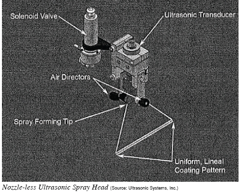
The Nozzle-Less Ultrasonic Spray Technology Difference
The technology that produces a spray with the desired properties for the application of the dopant layer utilizes a nozzle-less ultrasonic blade head to produce a rectangular, lineal coating deposition on the wafers. This deposition technique uses ultrasonic energy to break up liquid into very small drops coupled with a low-pressure air stream to shape the spray pattern produced by the ultrasonic spray head. The blade head assembly consists of an ultrasonic transducer with a spray forming tip, an external liquid applicator, air directors, and an ultrasonic generator.
Spray Pattern and Drop Size Distribution
The liquid is fed directly to the rectangular, vibrating spray forming tip of the spray head via the liquid applicator, where it is subsequently delivered to the entire surface. The liquid forms a thin film on the vibrating tip of the spray head and the ultrasonic vibrations form capillary waves in the liquid film. The ultrasonic vibrations then break the capillary waves into small drops, which are propelled from the spray forming tip in a flat, sheet-like pattern. Air directors produce air streams to expand the width and to gently accelerate the ultrasonically produced spray, creating a coating that is rectilinear in shape.
There are two important factors in producing a uniform coating layer:
1. Shape of the spray pattern
2. Uniformity of drop size produced within the spray pattern
However, the factor that most influences the uniformity of drop size is the film thickness of the liquid on the spray forming tip. The liquid applicator and the spray forming tip are specially designed to ensure that a uniform liquid film is delivered to the spray forming tip.
Liquid Delivery System
The dual precision metering pump liquid delivery system consists of a PFA reservoir to store the liquid dopant, two servo-driven positive displacement metering pumps, and flow control valves. The dopant in the metering pump is delivered to the spray head by the positive displacement of the piston. When the head is spraying wafers, the spray on/off solenoid valve is activated and the servo drive moves the piston at the programmed speed. The dopant flows from the metering pump to a solenoid valve, then to the spray head. The piston is driven by a closed-loop servo drive to ensure consistent speed and, therefore, a uniform and stable liquid flow rate. For maximum system uptime, two continuous-operation pumps ensure that dopant flow to the spray head is always available, allowing for high-volume production.

Coating System Platform
The coating system platform utilizes a self-cleaning, non-metal mesh belt conveyor to transport the wafers and servo-driven traversing mechanism for the ultrasonic blade head. The mesh belt, constructed from Teflon�� coated Kevlar��, is compatible with all currently available dopant formulations for maximum flexibility. The conveyor cleaning process utilizes a water-based cleaning bath to remove the dopant from the mesh belt and an air blow-off and IR drying module.
The conveyor width is 914 mm, accommodating up to 6 rows of 125 mm wafers, while the transport speed is adjustable up to 1.8 m/min. The maximum production capacity is 4,300 wafers (125 mm size) per hour at a conveyor speed of 1.8 m/min, meeting high volume requirements.
Coating Application Process Explained
The coating application process consists of three steps: the spray stroke, the return stroke, and the dwell period.
During the spray stroke, the spray head starts from the ��home�� position and traverses across the moving conveyor with the spray activated. The spray head applies a rectilinear coating pattern equal to the width of the wafers on the conveyor. The traverse speed for the spray stroke can be up to 2,000 mm/sec.
Once the head reaches the programmed process width, it immediately returns to the home position with the spray deactivated; this is the return stroke. The head waits at the home position until the wafers have traveled a distance equal to the programmed coating segment width, which is the dwell period.
Double Overlap Application Sequence
The actual width of the spray pattern produced by the ultrasonic blade head is approximately 152 mm, making it possible to apply the dopant to a row of wafers with a single spray stroke. However, this requires that the wafers be precisely lined up on the conveyor in even rows with a specific spacing, which, in post production facilities, is not realistic. In order to provide a uniform application of dopant on wafers, the double overlap application sequence is utilized. With this technique, a spray stroke is initiated at an interval equal to one half of the actual spray pattern width, optimizing the system for real-world manufacturing environments.
Uniformity of Dopant Application
The uniformity of dopant application to the wafers is affected by several factors, including the uniformity of the spray pattern produced by the ultrasonic blade head, the consistency of the traversing speed of the spray head, and the stability of the liquid flow rate.
The traversing speed of the spray head and the liquid flow rate are both controlled with closed-loop servo drive systems, so the variation in head speed and liquid flow rate is negligible. The uniformity of the spray pattern is more difficult to characterize, due to the small amount of liquid being applied to the wafers. The uniformity across the width of the spray pattern can be characterized visually, by inspecting the coated area of a single spray application. The uniform, rectilinear coating pattern, in conjunction with the double overlapping application sequence, yields a coating deposition variation on the substrate of ��5%, or better.
The formation of selective emitters represents an important advancement for improving solar cell efficiency. A critical factor for the successful implementation of this process for production is the ability to apply a uniform layer of liquid dopant to the surface of the silicon wafers. The new technique using a ��nozzle-less�� ultrasonic spray head with a precision delivery system platform that offers high-volume production with little waste, minimizing many of the concerns inherent in existing doping methods.
Stuart Erickson is President of Ultrasonic Systems, Inc. (www.ultraspray.com).
REFERENCES
1) Lasers in Solar Cell Production. Dave Clark, Newport Corp./Spectra-Physics. Of--October 2009, Photonics Spectra �� Laurin Publishing.
2) Laser-assisted selective emitters and the role of laser doping. Colville, F. Photovoltaics, 2009.
For more information, please send your e-mails to pved@infothe.com.
��2010 www.interpv.net All rights reserved.


.jpg)