By Darren Brown
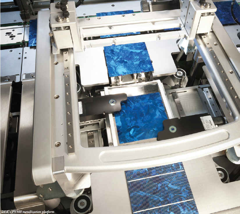
Photo by DEK Solar
 At the heart of over 90% of the solar cells manufactured today are sensitized silicon wafers, that capture incident sunlight and turn it into electrical energy. This is harvested and routed off the cell. It sounds simple enough, doesn’t it? And yet within this process lies one of the solar industry’s biggest ironies. And this is that the silver grid and bus bars that gather the energy and take it off the cell are in fact printed on top of the light-sensitive wafer, blocking sunlight from reaching it and rendering it partially incapable of doing what it was designed to do. At the heart of over 90% of the solar cells manufactured today are sensitized silicon wafers, that capture incident sunlight and turn it into electrical energy. This is harvested and routed off the cell. It sounds simple enough, doesn’t it? And yet within this process lies one of the solar industry’s biggest ironies. And this is that the silver grid and bus bars that gather the energy and take it off the cell are in fact printed on top of the light-sensitive wafer, blocking sunlight from reaching it and rendering it partially incapable of doing what it was designed to do.
There are clearly a number of excellent technological reasons for printing the energy-gathering grid on the front side of the cell, but this practice does present the solar industry with a significant challenge. And it is a challenge that cannot be ignored, especially considering that, even if some of the best cells are currently capable of harvesting in excess of 24% of incident sunlight, the industry standard for cell efficiency is around 16-18%.
Increasing Aspect Ratios
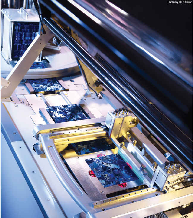
It comes as no surprise then to learn that the industry has done a great deal to reduce the size of the energy-collecting features. Currently grid line widths are in the region of 80-120 μm, and this is expected to drop still further to 50-60 μm in the immediate future, reducing the shadow effect and improving cell performances considerably while saving on materials costs. This is not without its complications, however. A conductor’s current-carrying capacity is directly proportional to its cross sectional area, so it follows that as its width is reduced, its height must be increased, yielding conductors with a higher aspect ratio. (A/R is measured as Height/Width. Standard aspect ratios today are in the order of 0.2 - 0.3.) This issue has been taken to heart by the solar industry, and special materials are available that improve high aspect line quality significantly. Several deposition methods, described in numerous papers, have also been developed for creating higher finer conductors. They include high precision mesh screen printing, metal stencil printing, metal jetting and even light induced electroplating. Perhaps one of the most promising, however, is a new metallization process that is already being used by a number of cell manufacturers, which could deliver aspect ratios that, at between 0.4 and 0.5, were until now impossible.
Print on Print
Print on Print (PoP) is not a new idea, indeed, it has been used in other industries for years. Simply put, and as the term suggests, this technique involves the printing of one conductor grid directly on top of a previously printed and dried grid.
Essentially there are two ways in which this can be done.
Top printing
In this case, the first, or base, print pass creates a grid pattern that is relatively wide and that stands relatively high. The second print, which is lower and narrower, sits directly on top of, and within the confines of, the base print without coming into contact with the silicon wafer. Clearly this requires extremely precise print alignment.
Encapsulation
Here, the base print pattern is low and narrow, and the second print pass is wider and higher. This top print pattern sits ‘over‘ the first, effectively encapsulating it and contacting both the first print pattern and the silicon wafer. While this approach still requires extremely precise printing capabilities, it is slightly simplified as the second print, like the first, has its confines on the wafer rather than on the base print pattern. For this reason, this encapsulation approach is thought to create a somewhat finer line, enabling widths of 60 to 70 μm to be achieved.
In the PoP procedure for the semiconductor and biomedical sectors, repeatable accuracy is key in both cases. Primarily because without it, this degree of fine line work would simply be impossible. Furthermore, misalignment can wipe out the advantages of fine line PoP work by increasing line width and, therefore, increasing the shadow effect. In the Top Printing approach, accuracy is even more of an issue if we consider that the landing area for the second printing pass, which is formed by the base pattern, is extremely limited.
Conducting Uniformity
 Printing onto a printed base pattern is also complicated in terms of gasketing, as DEK’s Senior Process Development Specialist Tom Falcon discovered when his team embarked on an in-depth study on the ways in which the efficiency of printed frontside silver conductors could be improved. The results of this ongoing work were first presented by Falcon in Hamburg at the 2009 European Photovoltaic Solar Energy Conference. One of the many issues that emerged from the study was that, as the aspect ratio of printed features rises, the wire in the printing screens tends to become increasingly obstructive, preventing the paste from properly filling the apertures, and it can even pull paste away from the apertures. The resulting conductors are uneven in height along their length, making them less efficient than a uniform conductor would be. This was graphically visible in the team’s analysis, which showed that the intervals between the highs and lows in any conductor mirrored the intervals between the knuckles in the screen mesh. The industry has done a lot to reduce this problem, with today’s 20-25 μm standard wire diameters contributing to improved aspect ratios and conductor uniformity. It is also possible to optimize screen emulsion thickness in order to achieve the best paste release properties for a given feature size, and paste manufacturers have done a great deal to improve silver paste formulations for high aspect ratio conductors. This notwithstanding, however, the non-uniformity issue still persists. Essentially this means that a manufacturer aiming to create PoP cells by using the top printing approach described above must not only center an ultra fine print pattern onto another, but must also create an effective gasket between the printing screen and a base pattern that is far from uniform. A tall order indeed. Printing onto a printed base pattern is also complicated in terms of gasketing, as DEK’s Senior Process Development Specialist Tom Falcon discovered when his team embarked on an in-depth study on the ways in which the efficiency of printed frontside silver conductors could be improved. The results of this ongoing work were first presented by Falcon in Hamburg at the 2009 European Photovoltaic Solar Energy Conference. One of the many issues that emerged from the study was that, as the aspect ratio of printed features rises, the wire in the printing screens tends to become increasingly obstructive, preventing the paste from properly filling the apertures, and it can even pull paste away from the apertures. The resulting conductors are uneven in height along their length, making them less efficient than a uniform conductor would be. This was graphically visible in the team’s analysis, which showed that the intervals between the highs and lows in any conductor mirrored the intervals between the knuckles in the screen mesh. The industry has done a lot to reduce this problem, with today’s 20-25 μm standard wire diameters contributing to improved aspect ratios and conductor uniformity. It is also possible to optimize screen emulsion thickness in order to achieve the best paste release properties for a given feature size, and paste manufacturers have done a great deal to improve silver paste formulations for high aspect ratio conductors. This notwithstanding, however, the non-uniformity issue still persists. Essentially this means that a manufacturer aiming to create PoP cells by using the top printing approach described above must not only center an ultra fine print pattern onto another, but must also create an effective gasket between the printing screen and a base pattern that is far from uniform. A tall order indeed.
Optimizing Printing Pastes

A great deal of work is consequently underway by materials and equipment suppliers to improve deposition performance. Paste manufacturers, for example, have developed dedicated pastes for the two separate passes: the base pattern paste is designed for low electrical resistance to the silicon layer, while the top pattern paste provides optimum electrical conductivity. Both paste types can be optimized for high aspect ratio printing.
...and Printing Screens
Screen manufacturers, too, have done a great deal to improve printing uniformity, but there is a limit to how fine wire meshes can go without using special but prohibitively expensive materials, especially given that they need to be robust. Screens for standard solar cell manufacture, for example, are typically expected to withstand up to 10,000 passes of a high-speed high pressure print squeegee without distortion or breakage. And when we talk about distortion, we are talking about micrometers--the brief is to keep the print screen’s dimensions, from corner to corner of a 15.6 cm wafer, to within a tiny ±10 μm!
The challenge becomes particularly clear if we consider how a printing screen is produced. Typically, the heart of the screen is made of a piece of woven steel fabric that is stretched and glued to a metal frame, then coated with a layer of photosensitive emulsion. This is then exposed, through a patterned phototool, to UV radiation that polymerizes the exposed emulsion. The remainder remains soluble, and is washed off in water, after which the screen is dried. It may then be put into a cardboard box, flown halfway round the world, and go through substantial temperature changes en route before being fitted to the printer. It may be handled carelessly, distorting the mesh or even the frame. The mesh wires may move within the screen structure as tension is applied and relaxed. Ambient temperature and humidity will affect the dimensions of the screen and the phototool in real time... the list goes on. The upshot is that there is a very real risk the pattern that is finally fitted to the printer is in some way out of true.
These issues become even more critical when we deal with not one, but two printing screens, that must be aligned not only to the silicon wafer, but also to each other. And that’s before you even start printing--the wear and tear to which a print screen is exposed during its working life is considerable, and can cause loss of tension in screens, resulting in image stretch.
Yes, there are considerable technical challenges inherent in PoP manufacture, and the industry is working hard to alleviate these. In Hamburg, Falcon presented an alternative print screen that is currently under development at DEK, which is essentially a hybrid alternative that combines the advantages of conventional print screens with those of meshless electroformed stencils. This could conceivably be a future solution for high aspect ratio print patterning.
In the meantime, DEK’s work to date indicates that PoP, which is now being adopted by a number of manufacturers worldwide, can practically be dropped in to any existing production environment at minimal cost, as long as the manufacture has excellent process control, uses quality printing screens, and can guarantee repeatable accuracy and precision in its printing processes.
Darren Brown is Global Business Manager for DEK’s Alternative Energy Group (http://www.deksolar.com/).
For more information, please send your e-mails to pved@infothe.com.
ⓒ2010 www.interpv.net All rights reserved.
|


.jpg)