Figure 1. Superconducting magnet system for crystal growth (1987)
By Arnaud de Potter, Bernhard Fischer
Silicon is currently the most common material used to manufacture photovoltaic cells. It is obtained by reduction from silica, the most abundant compound in the crust and especially in sand or quartz. The first step is the production of metallurgical-grade silicon, 98% pure only. The solar-grade silicon must be purified to more than 99.999%, which is obtained by converting silicon into a chemical compound to be distilled and then reprocessed into silicon. The resulting silicon allows to produce three types of photovoltaic cells.
The amorphous silicon cells are obtained by projecting, on a sheet of glass, a gas produced during the processing of silicon. The cells operate with a low or diffuse illumination and can be integrated on flexible or rigid substrates. Having a low efficiency, it would need to cover larger areas than when using crystalline silicon.
By the Czochralski method, the molten silicon is solidified by forming a large single crystal. Then the crystal is cut into thin wafers that give monocrystalline silicon cells. Having the higher yield, the monocrystalline cells have unfortunately the higher production cost.
During the cooling of silicon in a mold by the directional solidification process, the silicon solidifies to form an ingot consisting of several crystal grains. The ingot is then cut into blocks and each block is cut into wafers that give multicrystalline silicon cells. The ingot is a bit cheaper to produce than the monocrystalline ingots. The multicrystalline silicon cells also present an efficient conversion but slightlty less than for the single crystal.
The materials and manufacturing processes are the subject of ambitious research programs to reduce cost of ownership and recycling of photovoltaic cells. The industry seeks to reduce the amount of silicon used, to reduce the overall production costs, and increase efficiency and lifetime of photovoltaic cells.
In this article, we focus on the monocrystalline cell efficiency, being a key factor of forthcoming worldwide market competition.
Monocrystalline Cell Efficiency
When silicon ingot is grown by the Czochralski method, the melt is contained in a silica (quartz) crucible. During growth, the walls of the crucible dissolve into the melt and Czochralski silicon, therefore, contains oxygen.
Oxygen impurities can have beneficial effects. Carefully chosen annealing conditions can allow the formation of oxygen precipitates. These have the effect of trapping unwanted transition metal impurities in a process known as gettering. Additionally, oxygen impurities can improve the mechanical strength of silicon wafers by immobilizing any dislocations which may be introduced during device processing.
However, oxygen impurities can react with boron in an illuminated environment, such as experienced by solar cells. This results in the formation of an electrically active boron-oxygen complex that detracts from cell performance. Module output drops by approximately 3% during the first few hours of light exposure. Therefore, the reduction of oxygen incorporation into silicon ingot is one of the most important targets of solar ingot quality improvement.
The oxygen concentration, in the Czochralski process, is modeled by the following transport-diffusion laws:

where, C0 is the oxygen atom concentration [# at. 0/m3], D0 is the molecular diffusion coefficient [m2/s], DA is the additional (or turbulent) diffusion coefficient due to flow oscillations [m2/s].
Along the crucible wall, the dissolution equilibrium concentration is imposed:
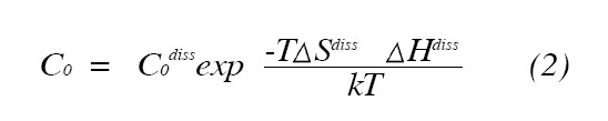
where Sdiss is the dissolution entropy [eV/K], Hdiss is the dissolution enthalpy [eV], C0diss is a consistency factor [# at. 0/m3], k is the Boltzman constant [eV/K], T is the temperature [K].
Along the melt free surface, equilibrium concentration with SiO concentration in the gas is imposed:
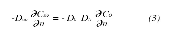
where CSiO is the concentration of SiO molecules in the gas phase [# molecules /cm3], DSiO is the diffusion coefficient of SiO in the gas phase [m2/s].
By representing the physics of the transport and diffusion in the Czochralski process, the above equations highlight three solutions to decrease the oxygen concentration in the silicon ingot.
Firstly, from equation 2, the hot zone can be modified in order to decrease the temperature of the quartz crucible. In such a case, the quartz dissolution is lower and the concentration of oxygen in the melt is lower. For decreasing the quartz dissolution, it is also possible to change the quartz crucible composition or to use a coating layer (equations 2).
Secondly, from equation 1, the operating conditions can be modified in order to change the melt flow pattern and to reduce the penetration of the oxygen in the crystal. The operating conditions can also be used to increase the oxygen evaporation along the melt free surface (equation 3).
Finally, the melt flow can be damped by using a magnetic field (equation 1).
In this article, we would like to highlight the advantages of the magnetic fields for growing low oxygen concentration ingot.
Advantages of Magnetic Fields on PV-grade Silicon Growth
Magnetic Device
The application of superconducting magnets to support the crystal growth process of monocrystalline silicon dates back to the mid 1980’s. The predecessor company of Bruker-ASC had built two solenoidal magnets providing a central field of 0.7 Tesla in a bore of about 600 mm. The magnet was built according to the available technology at that time, namely with a cryogenic liquid helium bath (LHe) which had to be refilled every several days (Figure 1) and with a helium gas cooled current lead. Nowadays a few features have changed and the magnet system turned to an “easy-to-manage” system.
Due to the well-established cryogenic technologies and the so-called high-temperature superconductor current leads the heat losses onto the cold magnet structure can be reduced tremendously. This given, one does apply fairly small cry-coolers to cool down the magnet system and keep it at operating temperatures of -269 or ~ 4 Kelvin in stand-alone mode. Going even further in cryo-technology the cold masses of CG magnets can be designed as so-called “try systems” This means that the magnet does not need any cryogenic liquids but one makes use of conduction cooling only. A customer, therefore, does not need to take care of any handling of cooling liquids, but instead all he has to do is--as with resistive copper coils--to plug the cryogenic system with its compressors and a vacuum pump to the electrical grid (and that’s it, see Figure 2).

Figure 2. Top view on a superconducting magnet system for crystal pulling (12″) with cryogenic system
In addition to the improvements on the cooling side, also the performance of the conductor materials and the tools for design have been developed further such that one can offer also much more complex magnetic field patterns than just axial fields from simple solenoids. It is well known from crystal growing processes for larger diameter, 12″ respectively 300 mm, that ingots for the semiconductor industry are requesting mostly a transversal field pattern related to the puller vertical axis (see Figure 3).

Figure 3. Horizontal magnetic field pattern of the magnet system in the center plane (crucible and ingot diameter are indicated) (Source: FEMAGSoft SA)
The typical field strength is in the order of 4,000 Gauss or slightly higher in the center of the crucible, which corresponds to a maximum field on the superconducting coils of nearly 50,000 Gauss (5 Tesla), a factor of about 12 larger, due to the large diameter of the crucible or the magnet coils, respectively. The directed horizontal field will exert forces on the melt flow to dampen the melt which has several positive impacts on the crystal growing process, especially much less oxygen content and lower surface tensions.
So called CUSP mode fields have been applied also to smaller crystal diameters in earlier days. For PV oriented crystals, on the other hand, the better results seem to be achieved with CUSP fields.
However, the ongoing simulations with different CUSP configurations in comparison to horizontal field patterns reveal also several positive impacts on the growing process for PV crystals with CUSP fields, as discussed within this article.

Figure 4. Magnetic field pattern within the crucible and ingot diameter and principle overview of a superconducting CUSP magnet system (8″) (Source: FEMAGSoft SA)
Simulation Software
In order to evaluate the potential of the magnetic fields on PV-grade silicon growth, simulation software such as FEMAG-CZ can be used. FEMAG-CZ, developed and commercialized by FEMAGSoft S.A. in Belgium, is a dedicated-software for the simulation of the crystal growth process.
Crystal growth simulations have recently attracted much attention and become an important part of the photovoltaic industry similarly to the experimental measurements employed for years.
The simulation software can, in general, predict the state of the crystal at any time during and after the growth. The state of the crystal is computed from the global temperature field in the growth system, the convection in the silicon melt and gas phase and conditions at the melt/crystal interface. Thermo-elastic stresses, the concentrations of impurities such as dopant, oxygen or carbon and evolution of crystal defects such as oxide particles and micro-voids in the crystal can be simulated.
Major advantages of the simulation software are:
1. To better understand the physics of the growing process,
2. To test any process set-up without physical implementation,
3. To find out the optimal process set-up parameters by a trial-and-error strategy performed on a virtual set-up.

Figure 5. Melt flow pattern during the growth of an 8″ diameter silicon crystal (24 inch diameter crucible). The stream function isolines are used to plot the melt flow pattern. The streamlines are tangent to the flow, or, in other words, the (u,v) velocity vectors are tangent to the streamlines. On the left side, the damping effect of a 1,500G CUSP field on the melt flow is highlighted. For confidentiality, the detailed of the hot zone used for the simulation cannot be disclosed. (Source: FEMAGSoft SA)
Virtual Experimentation
The simulation software was used to analyze the effect of a CUSP magnetic field on the Czochralski silicon ingot growth. Different hot zone configurations and operating conditions were used in order to model different growth set-up and to test the effects of several configurations of the magnetic fields (i.e., magnetic field intensity, magnetic field distribution, etc.) on the oxygen distribution as well as the pull speed capacity, energy consumption, solidification interface shape, thermal stresses and other key process parameters.
Four representative simulation results are described in Figure 5 and 6. The strong decrease, by about 50%, of the oxygen concentration in the crystal thanks to the magnetic field was highlighted. Moreover, the positive effect of the magnetic field on the pull speed increase capacity for a given hot zone configuration was emphasized. This is highly interesting for PV-grade silicon growth in order to increase the process yield.

Figure 6. Oxygen (# at./m3) during the growth of an 8″ diameter silicon crystal (24″ diameter crucible). On the left side, the effect of a 1,500G CUSP field on the oxygen concentration is highlighted. For confidentiality, the detailed of the hot zone used for the simulation cannot be disclosed. (Source: FEMAGSoft SA)
We would like to conclude this article by highlighting the high interest of the CUSP magnetic fields to address PV market challenges such as the growth of silicon ingot with a low oxygen concentration at a high pull speed.
Moreover, FEMAG-CZ simulation software has efficiently been used to predict and analyze the effect of the CUSP magnetic fields on the growing process performance. The software allowed to easily achieve first investigations and successfully provided key information for the development of this technology.
Arnaud de Potter is Head of Business Development at FEMAGSoft SA (www.femagsoft.com). Dr. Bernhard Fisher is Project Management & Engineering Magnet Systems at Bruker ASC (http://www.bruker-est.com/).
For more information, please send your e-mails to pved@infothe.com.
ⓒ www.interpv.net All rights reserved
|


.jpg)