By Andreas Weisheit
 The mass production of thin-film silicon PV modules is rocketing, generating economies of scale. In 2008, early adopters were achieving a cost of US$1.50 per watt, and this year, it has been predicted that the cost could drop to just US$0.70 per watt. Over the same period, manufacturing throughput is predicted to double, while materials costs will fall by around 50%. These factors are critical in the drive towards grid parity and widespread adoption of thin-film PV. The mass production of thin-film silicon PV modules is rocketing, generating economies of scale. In 2008, early adopters were achieving a cost of US$1.50 per watt, and this year, it has been predicted that the cost could drop to just US$0.70 per watt. Over the same period, manufacturing throughput is predicted to double, while materials costs will fall by around 50%. These factors are critical in the drive towards grid parity and widespread adoption of thin-film PV.
Fewer than 25 different gases and chemicals are used in solar cell manufacturing. This is relatively little in comparison with more than 50 required for semiconductors. Additionally, the volumes required are significantly greater and supply chain management presents its unique challenges. Among the direct materials for thin-film silicon in particular, glass and gases together can account for over 40% of the cost of solar module production. Therefore, while a 100 MW facility requires significant investment in infrastructure to ensure continuity of material supply, a 1 GW facility requires the entire output of an industrial-scale production facility for many of the principal materials.
Film Deposition
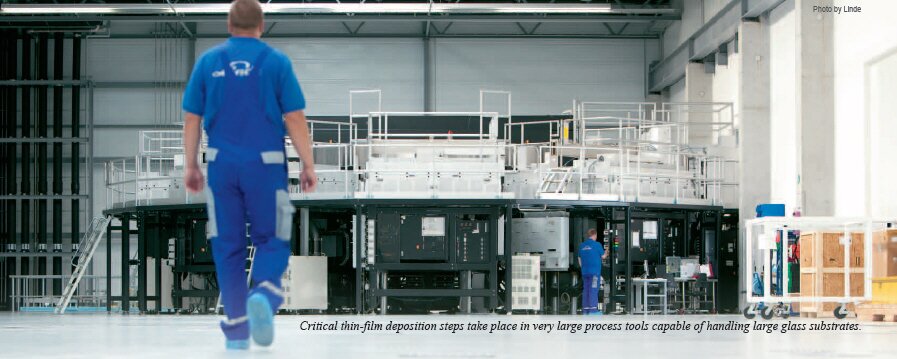
Electronic device manufacturing processes such as those used in thin-film PV are highly complex and multi-stage. The critical process step in all thin-film silicon technologies is deposition of doped silicon film from a silane precursor in a Plasma Enhanced Chemical Vapour Deposition (PECVD) system. The result is a thin film of silicon on the glass. Typically, hydrogen is also introduced to control the kinetics of the film growth. Dopants are incorporated through precursors such as trimethyl boron (TMB), diborane (B2H6), phosphine (PH3) and methane (CH4).
TCO Coating and PVD Glass Coating
Another important step in the thin-film PV cell manufacturing process is the deposition of a Transparent Conductive Oxide (TCO) film on the front glass. This is typically tin oxide or zinc oxide deposited via sputtering or using an organometallic precursor such as diethyl zinc (DEZ). The application of a back contact metal layer by physical vapor deposition occurs during the PVD glass coating process. This uses argon for aluminium or silver sputtering.
Chamber Cleaning
Between deposition steps, the equipment chambers require cleaning, and this is carried out with a reactive gas containing fluorine atoms. The film deposition process also results in silicon deposition on other surfaces in the PECVD process chamber such as the showerhead and chamber walls, which must be periodically cleaning. Typically, a fluorine-based etch process using nitrogen trifluoride (NF3), sulphur hexafluoride (SF6) or pure fluorine (F2) is employed for this purpose.
Fluorine Vs. Nitrogen Trifluoride
To minimize costs and maximize efficiency─and to ensure an environmentally sustainable manufacturing process─on-site generated fluorine is the most viable solution for chamber cleaning. Compared with nitrogen trifluoride, the default chamber cleaning gas, pure fluorine is a much more effective cleaning agent. It can be broken down into more reactive compounds more quickly and with less energy than nitrogen trifluoride. This reduces the cleaning time by more than 60% and uses up to 60% less power in the process. Replacing nitrogen trifluoride, a greenhouse gas, with fluorine also helps reduce the manufacturer’s carbon footprint because of fluorine’s zero global warming potential.
Unique to fluorine is the way it is supplied ─the gas is manufactured on the customer’s site on demand by a compact, modular plant. The supply of on-site generated fluorine requires different project considerations vs. packaged material supplies to ensure proper footprint, utilities availability and expansion capability. Planning for safety is integrated with the end user and community at an early stage, and because the on-site chemical inventory is substantially reduced, there are fewer licensing issues to deal with. Finally, on-site generated fluorine minimizes the risk of supply chain and pricing volatility.
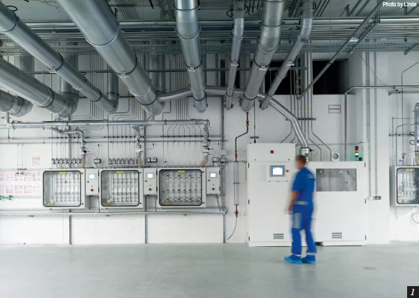
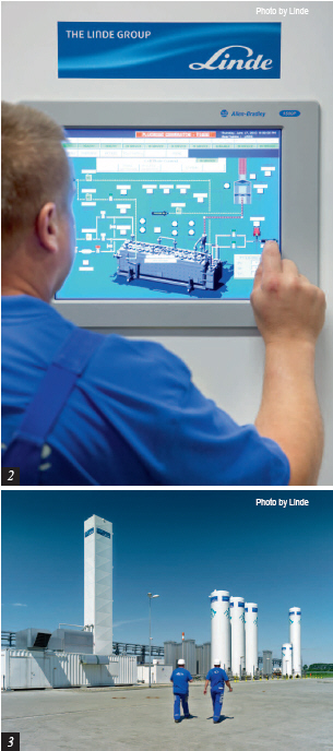
On-site generated fluorine is currently used in the commercial production of thin-film solar panels and other similar thin-film processes at many sites in both Asia and Europe. Production capacities ranging from 1 to 100+ tonnes per year have displaced high-pressure fluorine cylinder and bulk nitrogen trifluoride supplies. Overall more than 30 systems have been installed on customers’ sites in the TFT-LCD, semiconductor, and PV industries.
Dopant Gas Blending
As the scale of PV manufacturing increases, very high volumes of dilute dopant gases are required. A proprietary blending system which produces the dopant gas mixtures on-site brings customers improved security of supply and reduced transportation and change-out costs, helping to meet both carbon-footprint and cost-reduction roadmap targets.
Bulk Silane Storage
Silane is one of the most critical gases used for thin-film cell fabrication. Due to the large volume requirements─depending on the equipment between 150 and 300 kg per MW per year─silane is generally supplied in either multi-cylinder bundles or ISO modules containing up to 6000 kg. Given silane’s potentially hazardous properties, storage and delivery systems require careful design, installation and operation with all aspects of the bulk silane supply chain.
Bulk Compressed and Liquefied Gases
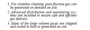
Aside from the electronic special gases and chemicals that are used, many more traditional industrial gases are required in both high purity and high volume. Thus a secure and reliable supply of these essential bulk gases, such as nitrogen, oxygen, argon, hydrogen and helium are demanded by thin-film silicon and crystalline silicon customers alike. These products are typically manufactured by global networks of high purity gas plants and delivered by road in liquid or compressed form to storage facilities on the customer site. Gas suppliers typically offer a design and installation service for bulk gas supply including storage tanks, evaporators, purifiers, filtration and corresponding ultra-high purity distribution systems. This ensures a safe and efficient operation with continuous product availability.
For very large volumes of some gases, notably nitrogen and hydrogen, an on-site generated solution is often the best supply option. In most cases, these are pre-packaged plants of well-proven design. For nitrogen, a cryogenic air distillation process is employed, while for hydrogen, steam methane reforming is a commonly used technique.
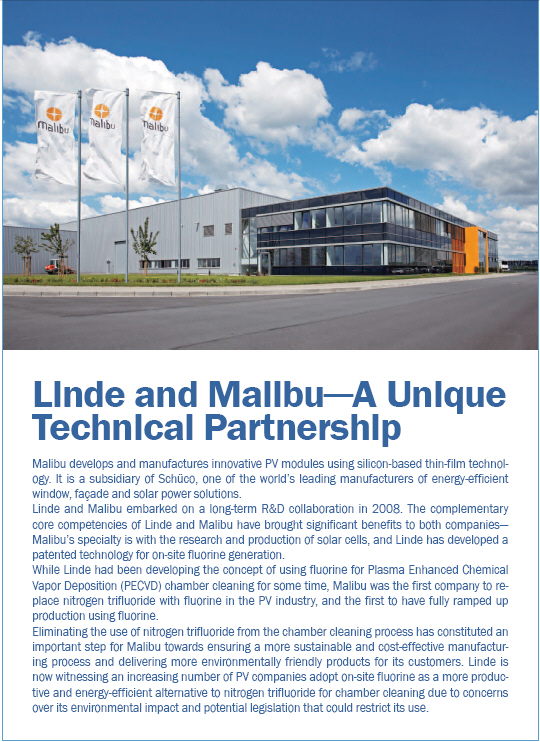
New Challenges
Gas suppliers are evolving from ‘traditional suppliers’ to integral parts of the manufacturing industry as PV manufacturers seek strong, reliable and knowledgeable partners with expertise in the wide range of specialist materials used in the thin-film silicon production process. As the industry grows, other challenges for manufacturers include managing safety and environmental issues, and developing materials technology that will both reduce costs and increase cell efficiency.
Andreas Weisheit is the Head of Global TFT-LCD & Photovoltaic Market Development at Linde Electronics (www.the-linde-group.com). Weisheit is responsible for global strategy, roadmaps, forecasting and business development for PV and the TFT-LCD industries worldwide. He is also responsible for all Asia market and business development in other electronics segments such as semiconductors and LEDs.
For more information, please send your e-mails to pved@infothe.com.
ⓒ2011 www.interpv.net All rights reserved. |


