By Ken Nauman, Skip Larson

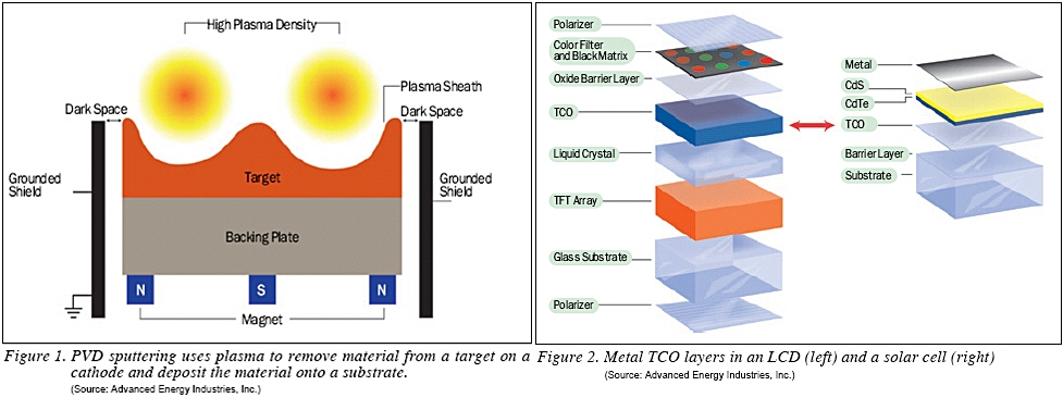
PVD (sputtering) is a common deposition method for thin-film manufacturing that uses plasma to remove material from a target on a cathode and deposits the material onto a substrate (Figure 1). In recent years, thin-film solar has leveraged time-tested plasma processing developments from flat panel display manufacturing. Similar materials are deposited in both applications, including metals, dielectrics, and TCOs. This article focuses on Direct Current (DC) sputtering for thin-film solar applications and how power delivery management can improve product quality and process control.
PVD Processing Fundamentals
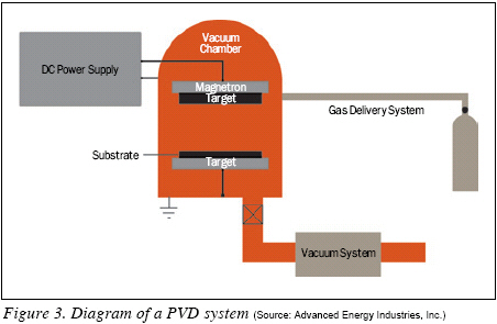
The magnetrons typically employ DC power supply technology for the conductive material deposition. The targets, consisting of either pure metals or ceramic compounds, are used to deposit the layers similar to the layers in an LCD panel--that form the front contact and back contact layers of a thin-film solar cell (Figure 2).
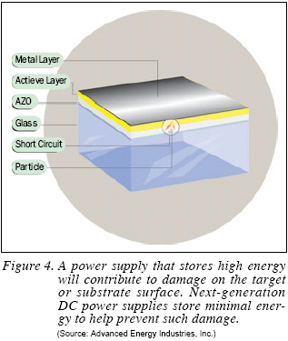
The metal layers make up the back contact electrical connection, so that light is reflected and resistance is minimized. The ceramic materials are Transparent Conductive Oxides (TCOs) used for the front contact electrical connection so that light is transmitted and resistance is low for efficient current conduction and reduced power consumption in an LCD or improved overall solar cell efficiency. To achieve minimum resistance and maximum yield, a film must be free of defects and pinholes, which are caused by arcs. A substrate (typically glass) is placed in front of the cathode, mounted in a vacuum system, for the deposition process. This can be a static process where the substrate is stationary or a dynamic process where the substrate moves continuously in front of the cathode. The major components of a vacuum system are shown in Figure 3.

Arc Management and Power Delivery
In any DC PVD process, charge buildup forms around inclusions or oxides on the target surface, which, upon discharge, results in plasma instability (arc). Although the power supply doesnt cause this charge buildup, effective arc management is required to mitigate any potential damage caused by the arc.
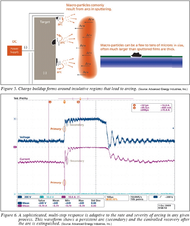
An arc is simply a charge buildup on a small area of the target with sufficient potential to cause an electrical breakdown. These low-voltage, high-current breakdowns eject fragments of the target material, which can manifest as defects on the substrate--leading to particle formation, pinholes, rate reduction, short circuits, or other undesirable process disturbances and loss of solar cell performance (Figure 4).
Arcing forms near insulative regions that are either inclusions in the target or debris on the target surface. These insulative regions will develop a charge buildup until sufficient to cause an electrical breakdown (Figure 5).
Due to the reactive nature of the process, arcing is a common occurrence in thin-film solar panel deposition of TCOs. For example, Aluminum-doped Zinc Oxide (AZO)--a transparent conductive oxide commonly used in solar cell applications--is known to arc hundreds or even thousands of times per second. It’s important nevertheless to maintain a high level of process control when depositing quality films to ensure deposition rate and film quality are preserved. High arc rates inhibit the creation of defect-free films and may prevent consistent deposition rate. Effective arc management is, therefore, a central topic of interest for solar cell process engineers performing thin-film deposition.
Power supplies must effectively manage arc events to minimize process disturbances and eliminate persistent arcs that damage the target or substrate. To extinguish an arc, the power supply needs to shut down or remove power from the output as fast as possible to limit the energy provided to the arc. Traditionally, power supplies used only voltage to detect an arc event, and the arc events were categorized as micro arcs or hard arcs. Previous-generation power supplies typically respond to an arc with this two-step approach. The initial response (micro arc) is very short, typically tens of micro-seconds. After the micro arc shut-down time, power is re-applied to the magnetron. If the arc persists, this is treated as a hard arc and the power supply shuts off for a much longer duration. The response to either step is as fast as possible, the only difference being the length of shut-down time. The energy delivered to the arc is dictated by the energy stored in the output of the power supply plus the energy stored in the cabling.
The latest-generation DC power supplies move beyond conventional micro- and hard-arc distinctions with increasingly sophisticated arc handling. New power supply designs store less energy, take a multi-level approach to arc response, systematically control power recovery, maintain a linear deposition rate, and are rich with custom process management options. Such advancements help quench arcs at high power levels--without compromising deposition rate and consistency--and thereby prevent unnecessary process interruptions, film damage, and losses in productivity and throughput.
Advanced Power Supply Designs Store Extremely Low Energy
Damaging particles on a film result from high energy feeding into an arc event. The shut down of the power supply is intended to reduce energy delivered to the arc. The shut down should be long enough to let the surface cool so that power can be re-applied without re-igniting the arc. Therefore, applying less energy to the surface location of the arc event before an arc is extinguished reduces target and substrate damage. Architecturally advanced power supply designs incorporate fast, internal arc switches and minimize stored energy (expressed as mJ per kW).
A Multi-Level Arc Response Adapts as the Rate and Severity of Arcs Change
Over the life of a single target, the arc rate and the severity of arcs will change. For the most stable power delivery throughout the lifetime of the target and the process, a power supply should detect and appropriately respond to actual arcing conditions with fewer persistent arcs and without causing new arcs to occur.
During an arc event, a change in the plasma operating conditions (impedance) causes the output voltage to rapidly approach zero while the output current increases dramatically. New power supplies are engineered to carefully monitor voltage and current and to activate an immediate response once the voltage and/or current pass a specified threshold or set of threshold criteria.
A multi-level arc response is rapidly replacing the conventional micro- and hard-arc distinction. The primary response will always involve the removal of output power to reduce the amount of energy given to the arc. This time should be as short as necessary to provide continuous output power, yet long enough to quench most arcs. If the arc clears, no additional response is required. However, if the shut-down time in the primary response is insufficient to cool the surface of the arc location and an immediate arc follows (or previous arc persists), a secondary response should set in. If the arc remains persistent, the duration of the response becomes progressively longer, sometimes resulting in a short-circuit response, until the plasma stabilizes. This is a much more effective and flexible approach that adapts to any given process for better control. The purpose of the progressive off time is to ensure that the arc is extinguished while minimizing the plasma off time. This will increase the delivered power and throughput (Figure 6).
Controlled Recovery Minimizes Persistent Arcs
How the power supply re-ignites the plasma is also becoming more advanced to prevent new or persistent arcs from forming. Applying too much energy (overshoot--Figure 7) after an arc shut down can create a subsequent arc. Some new power supplies incorporate a soft-start feature that gradually ramps power after an arc response. This limits the total number of arcs and therefore the number of possible defects.
Maintaining Set Point While Controlling Responses to Arc Events
The power set point is a user-selected value to provide the necessary film thickness. In heavy arcing conditions, a power supply may shut down so frequently that the amount of actual delivered power falls below set point. Some power supplies can now automatically regulate delivered power to maintain the set point and the sputter rate, compensating for the cumulative off time through sophisticated algorithms. This ensures the same deposition rate at the beginning and end of target life, resulting in more linear deposition over the power supply operating range--critical to maintaining line speed and throughput for consist and homogeneous films (Figures 8 and 9).

Arcs are unavoidable in PVD sputtering, especially for thin-film solar cell manufacturing. However, when uncontrolled, arcing can damage the substrate, reduce yield by causing defects, and reduce throughput by limiting power.
Engineered to remove power quickly, store extremely low energy, and gradually ramp power after an arc event, the latest power supply technology ensures that the power supplies themselves do not induce any arcs. For those unavoidable arcs that the target or process materials generate, power supplies are quickly extinguishing them through sophisticated techniques for arc detection and advanced multi-level arc response. Innovative power supplies that incorporate these new arc-management technologies are helping solar cell process engineers to overcome many of the quality and process control challenges in thin-film solar manufacturing.
Ken Nauman received his BSPS and MSME from Colorado State University. He is a senior applications technologist at Advanced Energy Industries, Inc., Fort Collins, CO., the U.S.A.
Skip Larson received his BSME from the Colorado School of Mines and his MBA from Southern Methodist University. He is a director of business development at Advanced Energy Industries, Inc., Fort Collins, CO., the U.S.A.
For more information, please send your e-mails to pved@infothe.com.
ⓒ2010 www.interpv.net All rights reserved. |


.jpg)