By Bruno Diaz
In the south part of China, where the number of solar irradiation hours is close to 2,000 hours/year, the number of module manufacturing companies is growing partially encouraged by the Golden Sun Projects and future Feed-in Tariff expectations. Concretely in the province of Fujian, currently there are around 25 companies mainly producing crystalline silicon modules. One of these companies is Linsun Power Technology (Quanzhou) Corp. Ltd (LSP), who has been in operation since early 2008 with a capacity of 50 MW and a target capacity for 2011 of 150 MW. Even though the company has yet small size, it is very dynamic and highly involved in several R&D activities to develop specific machinery and new solutions for the sector. Besides, LSP collaborates with international centers in order to study solutions to enhance the efficiency of solar cells. One of the most promising collaborations is with the Consulting, Renewable Energy and Optic (CERO) group of University of La Laguna, in the Canary Islands, Spain, headed by Dr. Guerrero Lemus.
From first generation solar cells, which are those formed by single junction, the main scope of this collaboration, supported by the Spanish Ministerio de Educacion y Ciencia (Project ENE2010-14865/ALT), is to study in depth the doping process with rare earth of crystalline silicon solar cells in order to improve the efficiency of solar cells by combination with luminescent up- or down-converters, that has been recently widely studied and theoretically described by several authors. These types of cells have been included into the so-called third generation, which includes, among others, non-semiconductor technologies, quantum dot, tandem/multi-junction cells, intermediate band solar cell, hot-carrier cells, up conversion and down conversion technologies, and solar thermal technologies. The second-generation refers to ‘thin films‘ made by layering plastic or glass with photovoltaic materials.
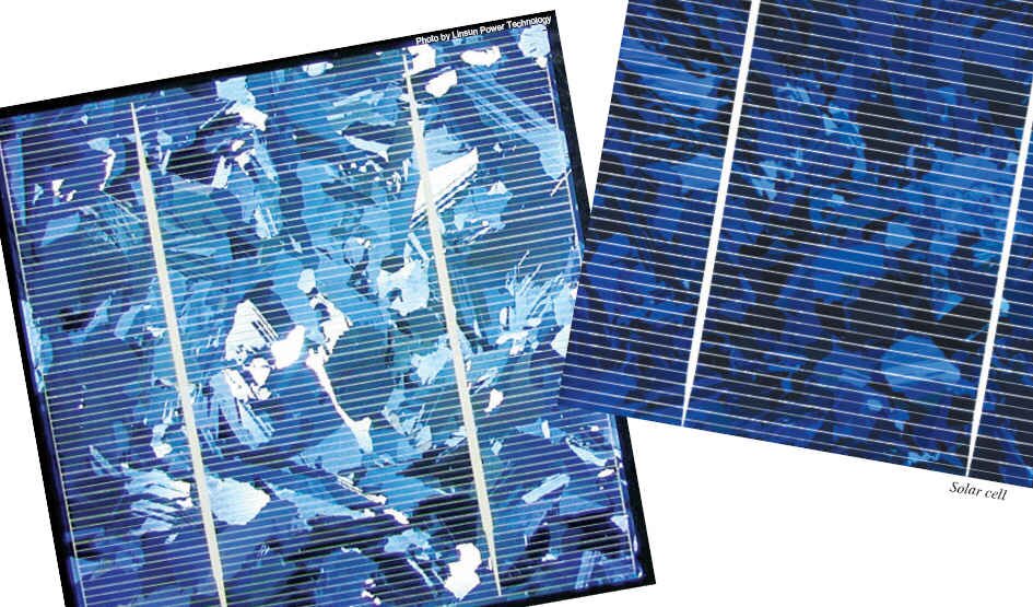
Porous Silicon Cells
Even though silicon is one of the most abundant elements on earth, it needs to be processed to be used in the electronic and solar industry by means of high energy consumption methods. Recently several proposals have been made in order to increase the relatively poor energy conversion of silicon photovoltaic solar cells. The essential difference proposed by this research is the low cost of the process as the doping process can be realized by adding one step to the process or using the same process used by the formation of the p-n junction. Moreover, it has been recently demonstrated that the down-shift contribution from the porous silicon layer could also be detected parallel with those from the up-conversion and down-conversion spectra of the added layers, which in this case are formed by rare earth combinations.
 Porous Silicon Layers (PSL) doped with rare earths have motivated several studies in the photovoltaic research community due to its light trapping, anti-reflection properties and light conversion ability. Recently, this conversion property has been added to other contributions mainly from rare earth or polymers incorporated to the cells or covering them forming a conversion layer. Therefore, the combined photoluminescence of the PSL and rare earths could enhance the efficiency of silicon solar cells due to the Down-Conversion (DC) and Up-Conversion (UC) processes from the rare earth alongside the Down-Shifting (DS) effect from the PSL. Porous Silicon Layers (PSL) doped with rare earths have motivated several studies in the photovoltaic research community due to its light trapping, anti-reflection properties and light conversion ability. Recently, this conversion property has been added to other contributions mainly from rare earth or polymers incorporated to the cells or covering them forming a conversion layer. Therefore, the combined photoluminescence of the PSL and rare earths could enhance the efficiency of silicon solar cells due to the Down-Conversion (DC) and Up-Conversion (UC) processes from the rare earth alongside the Down-Shifting (DS) effect from the PSL.
We can understand the importance of these conversion layers, if we study in detail the efficiency limits for any single-junction solar cell, which are the ones we all know in the market. This limit was calculated in 1961 by Shockley and Queisser according to the band gap energy (Eg) of the semiconductor from which the PV device is fabricated. Their calculation establishes a fundamental upper limit for the conversion efficiency of these devices. As a result, Shockley and Queisser demonstrated that the one-Sun efficiency limit for a single-material cell is around 31% with an optimal band gap of 1.3 eV. For the case of the silicon, with band gap of 1.12 eV the Shockley-Queisser limit is further reduced to 30%.
Due to its abundance in the earth, silicon is the most extended material in the semiconductor and PV industry. In terms of spectral irradiance, it has been calculated that the maximum power available for a silicon-based device is 468 W/m2. In addition, the maximum fraction of power available for down conversion processes is 149 W/m2 while the one accounted for up conversion processes is 164 W/m2.
Thus we have to overcome the problem that only photons with a wavelength below 1,120 nm are going to produce an effective electron-hope pairs. In particular, we account five main efficiency loss processes: lattice thermalization loss. transparency, recombination loss, junction loss and contact voltage loss. The two major loss mechanisms that need to be overcome to significantly enhance device efficiencies are the first two mentioned, which we can easily understand.
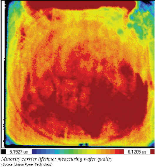
For the case of lattice thermalization, a photon with high energy creates an electron-hole (e-h) pair, however, the photo excited pair quickly loses energy in excess of the band gap and the extra energy is lost as heat within the device. The transparency of the semiconductor expresses the incapacity of these incident photons to create an e-h pair. This excludes a great portion of the infrared spectra. A further loss mechanism is the recombination of photo excited e-h pairs, however, the impact of this parameter can be minimized by maintaining high minority carrier lifetimes in the semiconducting material and does not contribute greatly to the theoretical efficiency limit.
Avoiding the Efficiency Loss
In order to maximize the efficiency, layers that could improve the photo conversion of naked silicon, would be added, attacking the described silicon weaknesses from different approaches.
In order to reduce the thermalization efficiency loss process, a Down-Converting (DC) layer can be placed on the front side of a silicon solar cell which would have the potential to generate more than one low-energy photon for every incident high-energy photon. The idea would be to use photons with energies over the band gap to produce photons of lower energies. It has been predicted a significant efficiency improvements will be possible also for non-concentrated sunlight for a solar cell in combination with a down-converter layers. A maximum theoretical efficiency of 38.6% was found for non-concentrated sunlight and for a converter with one intermediate level, which is a significant improvement over the Shockley-Queisser that we have already mentioned for all first generation solar cells.
The Promising Results Reached
 Besides, an up-converting material can generate one high-energy photon for every two or more incident low-energy photons. This material when placed on the rear side of a traditional bi-facial photovoltaic solar cell has the potential to increase the overall efficiency of the Photovoltaic (PV) device by absorbing sub-bandgap photons that would otherwise be transmitted through the device. Efficiencies up to 47.6% are theoretically predicted for non-concentrated sunlight for a solar cell in combination with such an improved up -converter. Besides, an up-converting material can generate one high-energy photon for every two or more incident low-energy photons. This material when placed on the rear side of a traditional bi-facial photovoltaic solar cell has the potential to increase the overall efficiency of the Photovoltaic (PV) device by absorbing sub-bandgap photons that would otherwise be transmitted through the device. Efficiencies up to 47.6% are theoretically predicted for non-concentrated sunlight for a solar cell in combination with such an improved up -converter.
Parallel, the application of a Luminescent Down-Shifting (LDS) layer has been proposed as a method for improving the poor spectral response of solar cells to short-wavelength light. The LDS layer absorbs photons, typically in the 300-500 nm spectral range and re-emits them at a longer wavelength where the PV device exhibits a higher response.
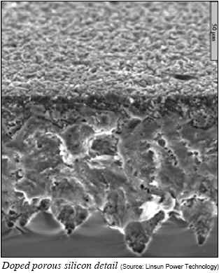
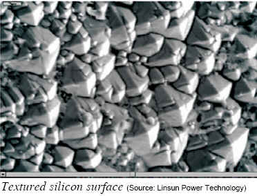
In addition, the simultaneous formation of a selective emitter may be achieved by converting into Porous Silicon (PS) the uppermost emitter cell region between the grid contact fingers. Chemical etching (also called stain etching) is more adapted to industrial fabrication due to its simplicity and lower cost. In this way, PS serves not only to remove the top emitter heavily doped dead layer but also acts as an antireflection coating and photo-conversion layer.
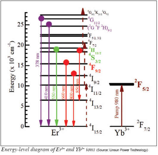
Based on the advantage of this low-cost and easy thermal doping technique, rare earths diffusion processes can be easily incorporated into solar cells production. Among rare earths, the Er3+ ion has concentrated large attention because of their emission in the Near Infrared (NIR) around 1,535 nm. The luminescence efficiency of Er3+ ion can be increased by co-doping with Yb3+ ion. Several authors refer to ytterbium as the adequate partner for erbium in order to enhance the poor absorption cross-section that shows the erbium at 980 nm. Furthermore, the observed quenching effect due to the auto-absorption of the Er ions and the presence of OH- ions has not been detected when co-doping with ytterbium.
The main issue when doping PSLs is the low thermal diffusion coefficient that remains unclear and obligates to high concentrations and long diffusion times at high temperatures, making the process a difficult task. However, PS, due to its known structure and high surface area, seems to be the ideal matrix in order to ease the penetration of the silicon by the rare earth ions.
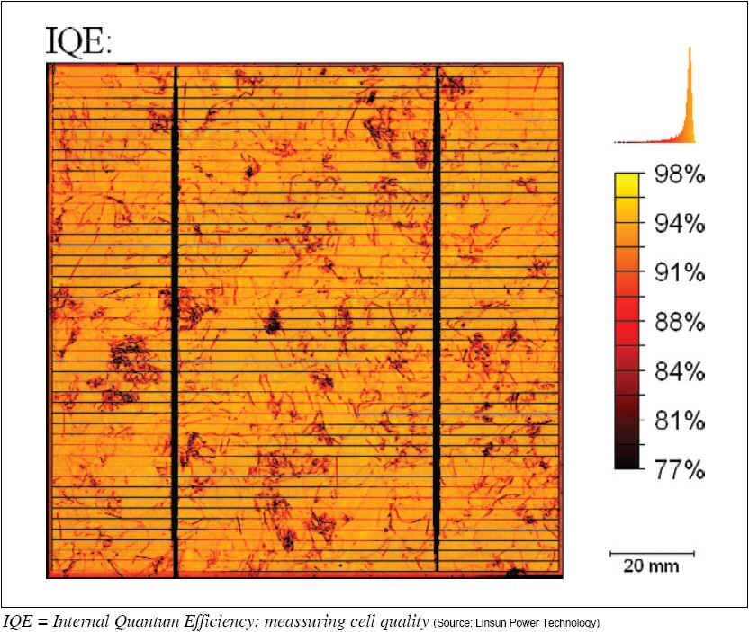
Though these techniques might increase the difficulty for the metallization process due to the roughness of the resulting surface, this can be considerably reduced after the doping processes to allow suitable front and back contacts via chemical processes, resulting in higher internal quantum efficiency that could boost the efficiency conversion of crystalline silicon solar cells. These energy conversion processes have also proven to be effective if applied to glass or EVA in the front side of the cell and in the EVA and back sheet in the rear part of the cell. Promising results reached encourage more in-depth research in this kind of field that could lead to surpassing the 30% efficiency barrier giving us a clear breach towards the challenging grid parity.
Bruno Diaz is an experienced technology executive with a rich history in production. Prior to working at LSP (www.linsun-power.com), Bruno Diaz, graduated in Physics, Industrial Engineer and Electronic Engineer with an MBA in Production and Manufacturing, he has been working for Siemens AG and ITER in the Canary Islands.
For more information, please send your e-mails to pved@infothe.com.
ⓒ2010 www.interpv.net All rights reserved. |


.jpg)