
By Henry Chou and Jeff Nestel-Patt
The process of growing multicrystalline silicon ingots used for manufacturing PV wafers is an immensely complex undertaking. The goal of the ingot growth process is to optimize mass ingot yield (amount of good waferable material produced) with throughput, and ultimately to produce material that can be made into high-efficiency cells to achieve a profitable operation. The ingot growth process requires careful monitoring and control of the myriad of variables within the directional solidification furnace during the crystallization process in order to achieve this goal.
Directional solidification furnace manufacturers are developing next-generation products to improve performance and efficiency of the ingot growth process. One feature that furnace manufacturers are investigating involves the ability to grow larger size ingots. There is a tendency to think that “bigger is better” and purchasers of capital equipment may be tempted by these claims. But is larger always better? This article explores some of the challenges associated with growing larger ingots and how they impact the economics of the ingot growth operation.
Understanding the Directional Solidification Process
Raw silicon used for producing PV wafers is grown in a highly controlled way during the ingot growth process to optimize grain structure and to ensure that impurities are segregated out of the melt before it solidifies into a multicrystalline silicon ingot. Better grain structure and fewer impurities means a higher quality ingot, which results in higher solar cell efficiencies and greater Megawatt (MW) output from a crystallization furnace.
Production of multicrystalline ingots is a batch process so it makes economic sense that processing more material per batch lowers the unit weight cost of the material. Over the past several years, production worthy furnace capacity has increased allowing ingots to grow in size from approximately 240 kg (gen 4) to approximately 450 kg (gen 5). As the size of the ingot has increased, the height of the ingot has remained relatively constant at about 25 cm to 26 cm.
Recently, several furnace suppliers have made claims that they have grown even larger ingots. Is this just the next step on the evolutionary path to a larger ingot? Is there an optimal ingot size? For example, to grow a 600 kg or larger ingot, the ingot can be wider, taller, or both. Let’s examine the potential challenges this imposes on the crystallization process and how these challenges impact the economics of ingot growth.
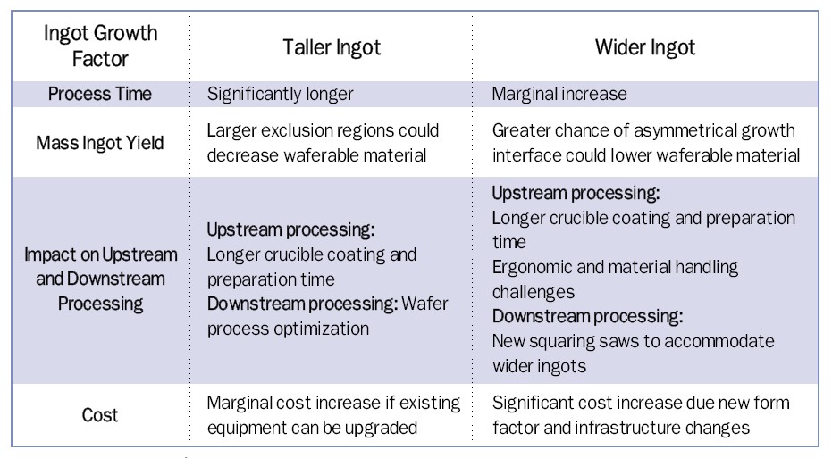
Figure 1. Ingot growth factor (Source: GT Solar)
Ingot Growth Economics
The ingot growth process is a capital intensive operation. Today’s high volume wafering facility may have up to 100 crystallization furnaces in operation. The continuing decline in module pricing is sending a profit margin shockwave through the entire PV manufacturing value chain requiring manufacturers to ensure that every node of their operation is returning value. While larger ingot sizes may seem like a solution to deriving more value from the capital equipment investment, wafer manufacturers should carefully examine four key economic factors that drive the greatest value before investing in the equipment necessary to start producing larger ingots. These factors are revenue/kg of material produced, mass ingot yield, throughput, and equipment price.
As was stated earlier, without becoming relatively taller, ingot sizes have steadily increased in width from 55 cm x 55 cm several years ago to the standard of 84 cm x 84 cm today. The wider ingot produces significantly more yielded waferable kilograms of silicon. The transition from gen 4 (240 kg) to gen 5 (450 kg) crystallization furnaces delivered measurable increased value to manufacturers when analyzed by the four key economic factors mentioned above. However, there may be practical limits as to how wide an ingot can be grown before the amount of yielded material diminishes to the point where it may increase the cost of the ingot growth operation.
Heating dynamics become more challenging as ingots get wider due to the increased distance between the center of the molten silicon and the hot zone heating elements located at the edges of the heating chamber. The greater the distance the more likely that the solid-to-liquid interface shape can become non-uniform resulting in less than optimal crystal growth from edge to edge of the ingot. As a result, mass ingot yield may be reduced because a greater percentage of the ingot can’t be turned into wafers due to the poor quality of the material. To address this problem, manufacturers could increase ingot growth times, but productivity would suffer because of the lower throughput.
Directional solidification furnace suppliers are also exploring the growth of taller ingots as a way to produce more waferable kilograms of silicon per batch. The height of the ingot can be constrained by the maximum cavity dimensions of the furnace hot zone so equipment modifications may be necessary. Like growing wider ingots, this approach sounds intuitive but producing taller ingots is not without its challenges.
Because directional solidification furnaces extract heat from the bottom of the crucible, raising the height of the ingot means heat must travel the extra distance through the additional material. If heat is extracted too quickly, the temperature
gradient between the top and bottom of the ingot will increase. This condition may lead to ingot cracking, causing a reduction in mass ingot yield. Furthermore, the additional time it takes for the heat to travel through the taller silicon mass will likely lead to longer batch processing times resulting in lower throughput. The increase in batch size and height must be intelligently balanced against cycle time to achieve a net throughput gain.
There are additional upstream and downstream production issues related to producing larger ingots that could impact operational costs that must be factored into furnace capital equipment purchasing decisions. Upstream, crucible costs will increase as they become larger and crucible preparation costs may also increase as the coating process becomes more complex. Downstream, larger squaring saws may be required to handle the wider ingots. Lastly, overall wafering productivity could decrease if line balancing between ingot growth and the sawing operation is not maintained. Producing more waferable material may increase throughput and utilization of the furnaces, but if the sawing operation can’t handle the increased material or form factor, a Work-in-Process (WIP) bottleneck or lower saw utilization could occur thus lowering the overall productivity of the wafering operation.
Value Metric
A useful tool to examine the economic impact of producing larger ingots is through the concept of a value metric. The major functional differences between furnace suppliers that impact the economics of ingot growth can be expressed as:

Here’s how the four primary criteria relate to ingot growth furnace economics.
Revenue/Kg
The crystal quality of a wafer contributes to the ultimate efficiency of a solar cell, and thus the efficiency of the module. Optimizing the amount of waferable material helps lower the cost of manufacturing, which in turn drives greater revenue for every kilogram of material produced.
Mass Ingot Yield
Described earlier, mass ingot yield is the waferable mass of the ingot after it is squared and cropped, divided by the weight of the charge prior ingot growth.
Throughput
Ingot growth furnace throughput is a function of ingot size and the time it takes to process raw polysilicon feedstock into a multicrystalline ingot. This can be expressed as ingot size divided by process time. This is usually expressed as kg/hr.
Equipment Price
This is simply the acquisition cost of the ingot growth furnace. When applying the value metric to compare the value of different suppliers ingot growth furnaces, usually the resulting annual depreciation expense is used, which is simply the equipment price divided by the depreciation period.
As manufacturers consider purchasing new directional solidification furnaces or upgrading their current systems to produce larger ingots, companies should carefully review the factors in the Figure 1 with their potential suppliers to help determine whether or not the transition makes economic sense at the present time.
Henry Chou is a Photovoltaic Equipment Product Manager at GT Solar (http://www.gtsolar.com/). He has over 17 years of product development experience with a number of high technology companies and has been awarded several patents in the semiconductor industry.
Jeff Nestel-Patt is GT Solar’s Director of Marketing and Communications and has held senior marketing roles in a number of semiconductor and high technology capital equipment companies.
For more information, please send your e-mails to pved@infothe.com.
ⓒ www.interpv.net All rights reserved
|


.jpg)