By Robert Pagliaro
.jpg) The new surface preparation criteria challenge the state-of the- art wet cleaning technologies that have been developed at world renowned institutions like IMEC and Tohoku University (Dr. Ohmi’s facility). Similar to the era when their ingenious cleans replaced the long running RCA cleans in the 90s, it seems apparent that significant changes may be required again to achieve these tougher specifications in the silicon-based PV and semiconductor manufacturing arenas. This article will demonstrate that simple but effective methods and enhancements can be used to not only achieve the more stringent surface preparation requirements but can also reduce complexity, cost of ownership and environmental concerns associated with the existing methods being used.
The new surface preparation criteria challenge the state-of the- art wet cleaning technologies that have been developed at world renowned institutions like IMEC and Tohoku University (Dr. Ohmi’s facility). Similar to the era when their ingenious cleans replaced the long running RCA cleans in the 90s, it seems apparent that significant changes may be required again to achieve these tougher specifications in the silicon-based PV and semiconductor manufacturing arenas. This article will demonstrate that simple but effective methods and enhancements can be used to not only achieve the more stringent surface preparation requirements but can also reduce complexity, cost of ownership and environmental concerns associated with the existing methods being used.
New Challenges for Silicon Device Wafer Wet Cleaning
For over 20 years, the leading-edge wet cleaning experts at the Ohmi and IMEC technology centers have continued to pave the way for achieving the surface preparation specifications required to keep pace with the advancement of silicon-based technologies. Current silicon-based technologies now demand surface contamination tolerances in the Parts per Trillion (PPT) regime, lower thermal budgets for processes like silicon epitaxy that require bake temperatures to be <800°C, and for silicon consumption per clean to be <0.1nm.
These new constraints may now surpass the capabilities of the best of class manufacturing cleaning sequences. Some of the key reasons are:
-The cleaning efficiency of their dilute chemistries, even combined with the use of tera-bit chemicals, may not be able to meet the ppt contamination requirements,
-A pristine and stable H-terminated silicon surface termination is required to enable the low thermal budget requirements for many thermal processes, and
-The use of peroxide and ozone-based chemistries inherently consume more than the 0.1nm of silicon per clean as defined in the ITRS roadmap.
Cleaning Efficiency
.jpg)
Most of the current wet cleaning processes used in manufacturing environments still terminate the silicon with a native/chemical oxide layer. This native or chemical oxide harbors a dominant portion of post cleaning contamination. Much effort has been put into the purification of the traditional wet cleaning chemicals such as ammonium hydroxide, hydrochloric acid, sulfuric acid, hydrofluoric acid and hydrogen peroxide. Tera-bit grade chemicals are now readily available. Chelating agents and additives, like EDTA and TMAH, as well as surfactants are commonly used to reduce contamination in wet cleaning chemistries. The addition of H2O2, HCl and alcohols are also commonly used in dHF mixtures to suppress contamination. While these can be somewhat effective remedies, the main ingredient in these mixtures, Ultra-pure Water (UPW), still contains dissolved impurities which impregnate the chemical oxides or terminate on the silicon surfaces following the cleaning sequences. These contaminants are also very detrimental for both oxide (ozone or peroxide based mixtures) and non-oxide (dilute HF) terminating wet cleaning sequences.
Oxide and Hydride Silicon Surface Termination
.jpg) Oxide terminating cleans suffice for processes that don’t restrict a subsequent high temperature process and are tolerant to silicon loss, but this tolerance is becoming very limited. Even in processes where it is still acceptable, the dissolved impurities like oxygen (DO), carbon dioxide, Total Organic Carbon (TOC) and silica in standard UPW are still present and can have a detrimental effect on the oxide integrity and other electrical properties. The interstitial carbon can also be diffused into the silicon when thermally processed. Dissolved organics in UPW needs to be dramatically reduced to improve the purity of these chemically grown oxides.
Oxide terminating cleans suffice for processes that don’t restrict a subsequent high temperature process and are tolerant to silicon loss, but this tolerance is becoming very limited. Even in processes where it is still acceptable, the dissolved impurities like oxygen (DO), carbon dioxide, Total Organic Carbon (TOC) and silica in standard UPW are still present and can have a detrimental effect on the oxide integrity and other electrical properties. The interstitial carbon can also be diffused into the silicon when thermally processed. Dissolved organics in UPW needs to be dramatically reduced to improve the purity of these chemically grown oxides.
Hydrogen terminating cleans, which are now in higher demand, are far more challenging due to the difficulty in creating a pristine and stable H-terminated silicon surface. There are three primary hydride structures that are formed on the silicon surface (mono- , di- , tri-) all of which have different binding energies and mostly controlled by the silicons crystalline orientation. SiHx terminations are ideal for many processes due to their ability to be dissociated at low temperatures (500-550°C) which suits very well for thermal budgeting. A HF last process is currently the only viable method to achieving this with wet cleaning. The Ohmi and IMEC institutions have each defined what they believe to be the best wet cleaning sequences1) to achieve all of the silicon surface criteria, both of which are short sequence (2-4 steps), utilize ultra-dilute chemistries and terminate with a dHF-based mixture. Both of these well-developed and characterized process sequences assuredly work well in a very controlled laboratory environment, but there are severe challenges when trying to implement these into a manufacturing mode:
-Achieving 100% SiHx terminations using a dHF wet cleaning process is virtually impossible
-Minimizing the queue time between the wet clean and the subsequent process is critical due to the inherent reoxidation of the silicon surface when exposed to air
-Exposure of the SiHx surface to air also permits for the adhesion of organic contaminants
Similar to oxide terminating cleans, the dissolved impurities in UPW have a dramatic influence on the dHF process’ ability to provide a pristine, stable H-terminated silicon surface.
Silicon Consumption
Meeting the ITRS surface preparation requirement of consuming less than 1A of silicon per clean poses the most difficult challenge for the wet cleaning gurus. A single monolayer of oxide growth triples this criterion. To remove metals, organics and particles without using either H2O2 or O3-based chemistries defies the current wet cleaning protocols. Even the best of breed IMEC and Ohmi cleans require the use of these oxidizers. Aside from something completely new in wet cleaning chemistries the only practical panacea seems to be to assure near 100% photoresist removal in the plasma ashing process and depend on a very pure and effective dHF mixture (with non oxidizing additives) to remove all of the contaminants.
Silicon Wafer Drying Methods Are also Challenged
Along with the new challenges with which the wet cleaning and rinsing steps are confronted, there is evidence that the current state-of-the-art silicon wafer drying methods which use IPA are now a source of unacceptable organic contamination levels. Detailed studies have been done to qualitatively and quantitatively assess this2). Residues following Marangoni and IPA vapor drying have shown to severely affect the electrical performance for gate oxides less than 5nm3). It is also counterproductive in that it can blanket the surface of the wafers after the H-terminated cleaning processes, which has a significant impact on critical front end processes like low temperature Si and SiGe based epitaxy, poly-Si stacks and metal deposition.
With the lowering of surface contamination specifications, the benefits that come with IPA assisted drying are being outweighed by the contamination levels of its post-drying residues. Other non-chemical drying methods need to be enhanced or developed.
Simple Enhancements to Achieve the Demanding Surface Preparation Requirements
.jpg) Now that the key issues with the newer surface preparation criteria have been identified, simple enhancements to the existing leading edge wet cleaning technologies that can help overcome these issues will be discussed. The core process engineering work and recipes that the Ohmi and IMEC camps have developed offer a great basis to build upon, but are not a complete set of instructions on how to make them work in a device manufacturing facility.
Now that the key issues with the newer surface preparation criteria have been identified, simple enhancements to the existing leading edge wet cleaning technologies that can help overcome these issues will be discussed. The core process engineering work and recipes that the Ohmi and IMEC camps have developed offer a great basis to build upon, but are not a complete set of instructions on how to make them work in a device manufacturing facility.
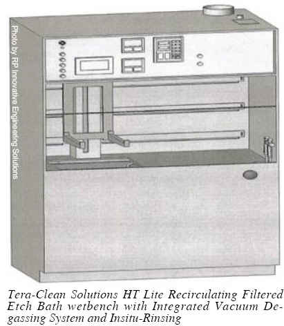
Thorough investigations on the growth of native oxide on silicon wafers4), 5) immersed in DI water with various dissolved oxygen levels and air (Figure 1) and as well as the benefits of functional H2 water on particle removal efficiency and hydrogen terminating surfaces6). Degassing and regassing of Ultra-pure Water (UPW) can become an integral part in achieving these new criteria. Integrating this with a dHF cleaning process has a dramatic effect on its capabilities. HF last wet cleaning processes, single and two step, have been patented7, 8) , which provide a pristine and stable H-terminated silicon surface with an extensive queue time and can be accommodated in a variety of wet processing equipment. Some of the key components to making this novel technology work are:
-Specific dHF chemistry and process conditions
-Ultra-degassed water (<100ppt)
-H2 functional water or anionic surfactant9) to achieve >90% particle removal efficiency)
insitu-rinse10), 11)
-Process equipment with high purity components and plumbing
XPS studies have demonstrated that this process7) can produce non-detectable oxide (<0.1A) for up to 3 days. Another extremely sensitive method to quantify the lack of C and O on the surface after the dHF process is encapsulated SIMS. The lack of oxygen and carbon for these two characterization methods are indirectly indicative of the degree of SiHx are on the surface after the wet cleaning processes (Figure. 2) Depending on the DO of the UPW, this process can yield aerial oxide densities <3E12 at/cm2 (Figure. 3). This capability has allowed for sub-800C thermal budgeting for low temperature Si and SiGe epi processes (Figure. 4). This process has also proven to allow for a queue time in excess of 8 hours without the use of special handling between the clean and the epi process.
.jpg)
.jpg)
.jpg)
There is evidence that dHF is very effective at removing organic residues, like BHT and DBP which outgas from plastic wafer shipping/storage boxes12). It also has been found to be especially good at removing oxidized polymers following plasma etch processes. So in many, if not most cases, it is now possible that a single step dHF wet process can be used to minimize silicon loss as well as lowering the cost of ownership and environmental issues.
To address the organic residue issue with using IPA for wafer drying, enhancing the capabilities of less effective methods like conventional Spin Rinse Drying (SRD) have been investigated and could be an acceptable option to replace the existing process of record IPA drying technologies.
Two enhancements to an SRD tool that could allow them to resurface as effective drying tools to meet the new surface preparation criteria are:
-Complementing the drying step with vacuum can significantly reduce water micro-droplets
-Utilizing low DO (degassed) UPW for the rinse has shown to eliminate water marks13)
.jpg) The reduction of micro-droplets and watermarks could enable an equivalent drying capability to the IPA-based dryers without the drawback of leaving organic residues.
The reduction of micro-droplets and watermarks could enable an equivalent drying capability to the IPA-based dryers without the drawback of leaving organic residues.
Last of all, a brief, low temperature treatment could be utilized for removing both the IPA residues as well as the airborne organic contaminants that accumulate on the wafer surface during between the wet cleaning step and the subsequent FEOL or BEOL process. It has been demonstrated that a 300-400。C bake with IR lamp heating for less than 2 minutes in an oxidizing environment can effectively remove both of these organic contamination sources14). A method has been developed that combines vacuum and IR lamp heating to assure the most effective decomposition and desorption of the organic species and moisture.
Although complex issues arise with the tightening of surface preparation specifications that come with the emerging PV and device technologies, it has been demonstrated that solutions can be simple in nature. Some examples of simple approaches to these dilemmas are:
-A single step dHF clean could accomplish overcoming the three identified hurdles associated with the new surface preparation criteria.
-Degassing the DO and the other dissolved species in UPW and chemicals has shown to be a valuable technique for dramatically reducing contamination levels in the cleaning, rinsing and drying steps of a wet cleaning process.
-SRDs could be enhanced for effective wafer drying and replace IPA-based methods
-Unavoidable airborne organic contamination and IPA drying residues can be nearly eliminated with a fast, reduced pressure, low temperature treatment.
These simple approaches to achieve the challenging surface preparation criteria can be found on commercially available equipment.
Robert Pagliaro received his BS in Physics from Thomas Edison State College (Trenton, NJ) and is Founder and President of RP Innovative Engineering Solutions, LLC (http://www.teracleansolutions.com/).


.jpg)